


CoAsia SEMI Becomes the First in Korea’s Design Service Industry to Enter 3D IC Package Mass Production
2026.08.11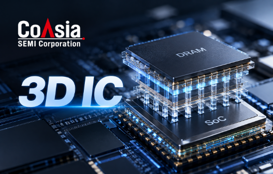
CoAsia SEMI announced on the 11th that it has begun mass production of a system-on-chip (SoC) featuring three-dimensional integrated circuit (3D IC) packaging.
3D IC packaging is a technology that vertically stacks multiple dies, such as DRAM and logic SoCs, using vertical interconnection technologies including through-silicon vias (TSVs). Compared with conventional 2D and 2.5D structures, in which memory and logic are placed side by side, 3D IC packaging can provide higher memory bandwidth and improve data movement efficiency, making it particularly well suited for emerging agentic AI applications.
Leading global semiconductor companies, including Qualcomm, are also strengthening their 3D IC capabilities to secure next-generation AI memory technologies.
The product that CoAsia SEMI has now entered into mass production applies the latest wafer-on-wafer (WoW) hybrid bonding technology, vertically stacking multiple customized DRAM dies on top of a logic SoC.
Compared with the CoW (Chip-on-Wafer) method, which stacks dies individually, the WoW approach significantly reduces the distance between layers and greatly improves large-scale data processing performance, according to the company.
Dong-soo Shin, CEO of CoAsia SEMI, said, “Another project applying 3D packaging is currently in the final stage of development,” adding, “We are also discussing development and supply cooperation with multiple global customers.”