


SoC Design Service
A Design Ecosystem
Expanded by Technology
Expanded by Technology
Semiconductor
Business Overview
CoAsia offers a comprehensive service spanning the entire semiconductor lifecycle, from specification to chip development and sales.
-
 AI
- Size30x40mm
- PCB Layers10L
- RDL interposer
-
 Data Security
- Size25x25mm
- PCB Layers8L
- System in Package
-
 HPC
- Size40x40mm
- PCB Layers12L
- HBM Integration
-
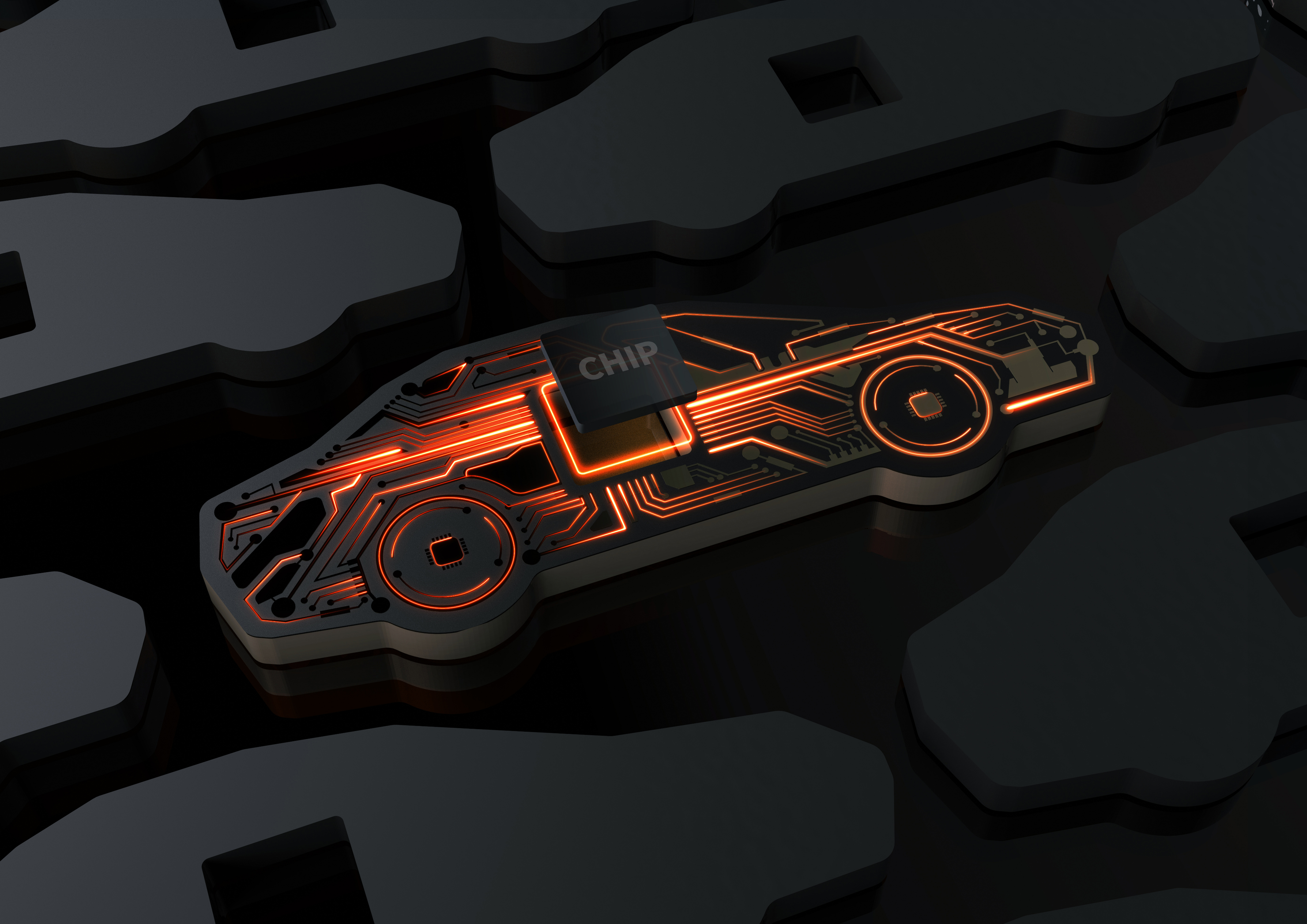 Automotive
- Size28x28mm
- PCB Layers10L
- ASIL-D Ready
-
 Robotics
- Size25x25mm
- PCB Layers8L
- Edge AI Package
Total solution provider

IDEA & SPEC
View More
Spec-in Design &
Verification View More Chip Physical Implementation View More Advanced PKG
Technology View More S/W Solution View More
Verification View More Chip Physical Implementation View More Advanced PKG
Technology View More S/W Solution View More
RTL Design Service
Physical Design Service
2.XD / 3D / Legacy PKG
Solution S/W + H/W Development
Solution S/W + H/W Development
SoC Design Service
PE&QA Service
PKG/Test Service
Supply Chain
Management
Management
Production Service
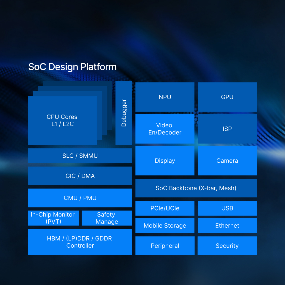
SoC Design
Providing high-reliability, silicon-proven SoC platforms built on cutting-edge process technologies and the latest IP integration

Spec-in Design&Verification
-
Spec in Design
- Accelerating TTM via silicon-proven SoC Design platform.
- Targeting High-Growth Verticals: Automotive, Vision AI, IoT, and HPC Multi-Die solutions.
-
SoC Design
- Full-stack turnkey services: From architecture spec to hardware validation and BSP/SDK deployment.
-
SoC Verification
- multi-level hierarchy using UVM and VIP-based methodology
- Quality sign-off through rigorous performance and power validation
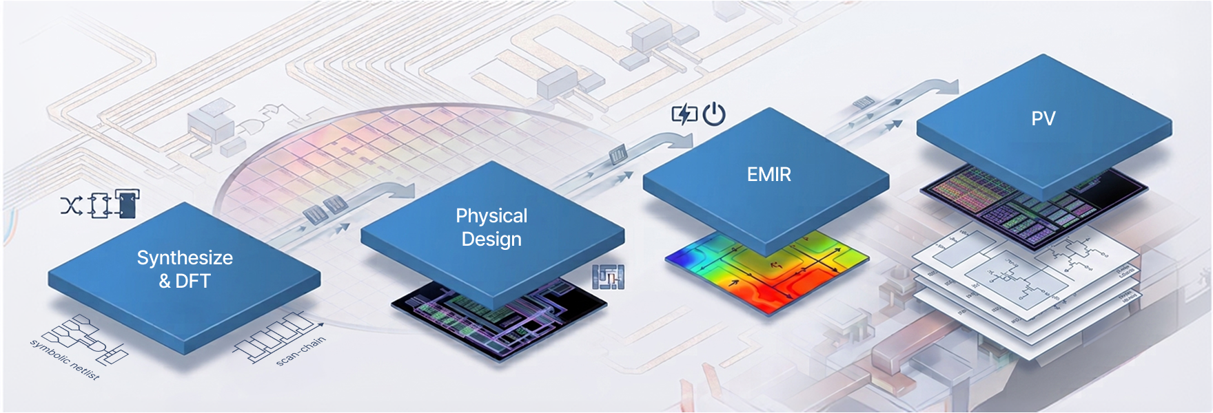
Chip Physical Implementation
Advanced Architecture to Silicon Proof:
Comprehensive SoC Sign-off Solutions
-
1Synthesize & DFT
- Physical aware Synthesis
- DFT : LBIST/ OST/ IST/ Cell-Aware ATPG
- Advanced Test Access : D2D/ Standards-based test access
-
2Physical Design
- Application based power-planning
- Advanced CTS (clock mesh/ Spine/ H-tree)
- Low power aware placement & routing
-
3EMIR
- Signal/ Power/ Bump EM analysis
- Chiplet(2.5D, 3D, 3.5D) level on-chip EMIR anlaysis
- Multi-domain Power Integrity Analysis
-
4PV
- DRC/ LVS/ DFM/ ESD
- Chiplet verification (2.5D, 3D, 3.5D)
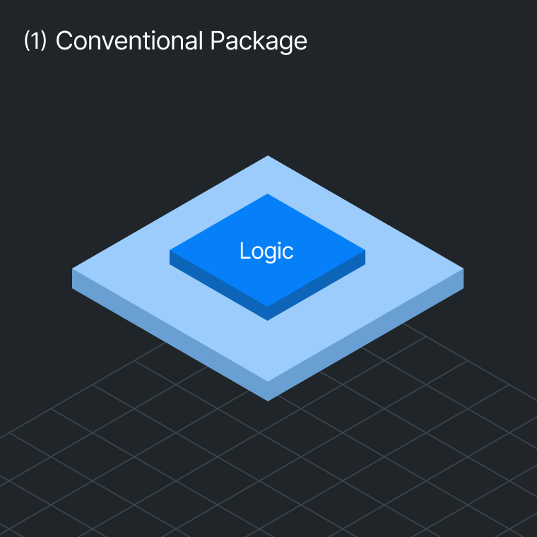
Advanced Packaging Technology to support
All-in-one-service for large scale PKG and High Bandwidth Memory
-
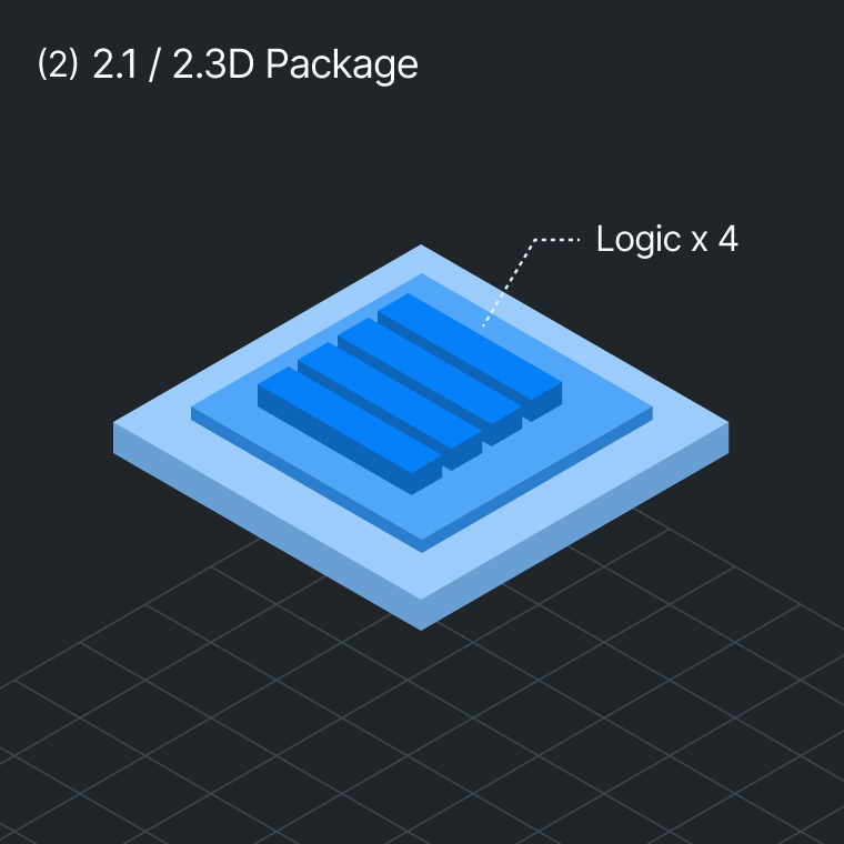
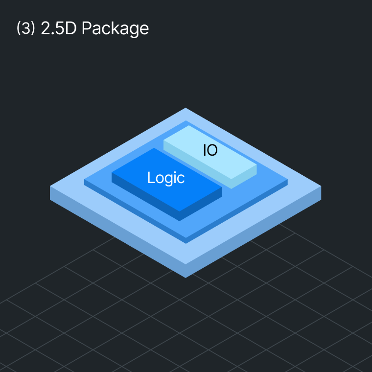
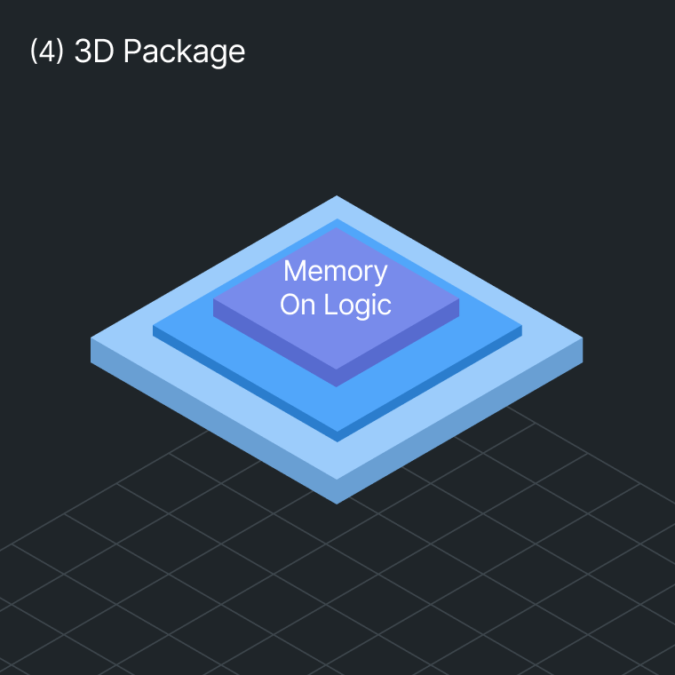
1PKG platform(2D~3D)
- Scalable solutions support (2.1D to 3D PKG) based on cost, manufacturing, and performance
- TTM acceleration through chiplet-based platform leverage
-
2Ecosystem
- Fully support 2.XD w/ Amkor and 3D w/ Winbond to satisfy PPA and high inference (Amkor, SFA, HANA Micron, DAEDUCK, DOOSAN)
-
3Advantage
- Shortest assembly plan (3 months) via secured design-level TAT
- 3-month schedule reduction through streamlined OSAT collaboration
Service Process
- Large reticle/body Substrate design
- PKG Structure simulation
- PKG material pre-order
- SIPI Sign-off
- PKG Ass'y
- Shipping
SW & HW Solution
Reliable SW/HW Solutions Built on Extensive OS/Platform Development and Mass Production Experience
Production-grade platform
software provider
software provider
· AP supply for over 4 million embedded products and Linux/Android BSP development for AP platforms







SLT
Specialist
Specialist
· Industry-leading capabilities in SLT SW/HW development
· Proven experience in operating SLT mass production lines since 2016